

Electrostatic discharge is the only failure mode in UAV electronics that can destroy a component without leaving a trace. A 2 kV human-body-model discharge, the low end of what a person feels, pushes about 1.3 A through a 1.5 kΩ source in under a nanosecond of rise time. CMOS gate oxides in modern flight controllers are a few nanometers thick and break down at single-digit volts. The result is a class of field failure that passes final test, flies for weeks, and dies on a cold dry morning when a technician plugs in a battery. The electronics manufacturing quality guide covers the assembly-side controls that prevent damage in the factory; this guide covers the design-side protection that keeps the aircraft alive in the field.
Why ESD is the silent failure mode in UAV electronics
ESD damage is invisible because it is statistical. A single discharge above the device's withstand level can punch through a gate oxide immediately, but far more common is latent damage: the oxide is weakened, the junction partially degraded, and the part fails weeks later under thermal or electrical stress. Industry estimates attribute roughly 20-30% of field-returned electronics to ESD-related damage. And on UAVs the number runs higher because the aircraft is handled constantly between flights.
- Charge generation is unavoidable. Walking across a carpeted room generates 1,500-35,000 V depending on humidity. Below 40% relative humidity, a normal winter or desert day, charge generation roughly doubles compared with 60% RH. Field operations, vehicle boots, synthetic clothing and dry air make a UAV ground crew a walking charge generator.
- UAVs are all interfaces. A multirotor has battery connectors, payload connectors, USB and SD ports, antenna feedlines, and exposed metallic airframe parts. Every one of these is a discharge path into the electronics, and most are touched during normal operations. The connectors and wiring guide details the harness side; this guide covers the protection at each port.
- Latent damage defeats quality control. A weakened gate oxide passes every functional test. The failure appears at altitude, under vibration and temperature cycling, where nobody can see it. That is why ESD protection belongs in the design, not in the warranty claim.
The failure signatures on UAVs are recognizable: intermittent flight controller resets, corrupted telemetry or log files, a GNSS receiver that loses lock permanently, an ESC that desyncs once and never again, a video link that degrades after a payload swap. If a field crew sees these symptoms after handling, the first suspect is ESD. And the fix is protection at the interface, not a replacement board.
Where ESD enters a UAV: the charge paths that matter
Protection starts with a map of every conductor that leaves the protected electronics. Each path needs a decision: is it exposed to handling, and what is the worst discharge it can see?
| Entry point | Typical discharge source | Result if unprotected |
|---|---|---|
| Battery connector (XT60 / XT90 / AS150) | Handling, mating in dry air, field swaps | FC brownout, ESC gate damage, PDB transient damage |
| Payload connectors (UART, CAN, Ethernet, PWM) | Hot-plugging payloads between missions | UART or CAN transceiver death, FC IO latch-up |
| USB and SD ports | Field laptops, memory card swaps, firmware updates | USB PHY damage, boot failure, corrupted storage |
| Antenna feedlines (GNSS, telemetry, video) | Antenna changes, coax handling, static on the element | LNA or RF front-end destruction, permanent link loss |
| Exposed airframe metal and mounting hardware | Charged airframe touching ground equipment or crew | Discharge through mounts into the ground plane, secondary damage to anything referenced to it |
The payload integration guide shows how many of these interfaces a typical mission stack has. Each one is a candidate for a TVS diode, an ESD suppressor, or a series element. And the selection depends on the signal it carries.
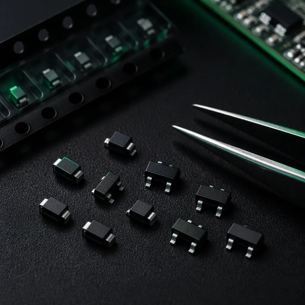 Protection devices
Protection devices compared: TVS diodes, ESD suppressors, polymer and spark gaps
Four device families cover almost every UAV protection need, and they differ in the trade-off between clamping voltage, capacitance and cost. The choice is dictated by the signal: a 1 MHz telemetry UART can tolerate a 30 pF diode; a DShot1200 signal line or a USB 2.0 pair cannot.
| Device | Clamping behavior | Capacitance | Best role on a UAV |
|---|---|---|---|
| TVS diode (unidirectional) | Sharp clamp at defined voltage, 100-600 W peak pulse | 5-50 pF typical; low-cap variants 0.5-3 pF | Power rails, CAN, UART, battery and payload connectors |
| TVS diode (bidirectional) | Symmetrical clamp for AC or differential lines | 5-50 pF | RS-485, Ethernet magnetics side, lines that swing both polarities |
| ESD suppressor array (multi-channel) | Steering diodes to rails, rail-to-rail clamp | 0.3-2 pF per line | USB 2.0, DShot, SBUS, video data lines, high-speed ports |
| Polymer ESD suppressor | Triggered switch, very low capacitance | <0.1 pF | RF and antenna feedlines where pF-level capacitance destroys matching |
| MLV (multilayer varistor) | Gradual clamp, higher leakage | 50-500 pF | Bulk power inputs; poor choice for signal lines |
| Spark gap / GDT | Arc discharge at high voltage, handles huge currents | <1 pF | Lightning indirect effects on large airframes; not for low-voltage logic |
The EMC/EMI design guide treats these devices as part of the immunity architecture. A TVS diode that clamps an ESD pulse also shapes conducted transient response, the two disciplines share the same components, and the same test chamber.
TVS diode selection for UAV signal lines: standoff, clamping and capacitance
Selecting a TVS diode is a three-number exercise: standoff voltage, clamping voltage, and capacitance. Each number maps to a design constraint, and getting any one wrong makes the protection useless or harmful.
- Standoff voltage (V_RWM). The maximum continuous voltage the line carries in normal operation, plus margin. A 3.3 V logic line with 10% tolerance needs a device with V_RWM around 3.3-3.6 V. A 5 V device will never clamp before the logic is damaged. For a 24 V CAN bus transceiver supply, V_RWM 24-26 V; for a 6S LiPo rail at 25.2 V fully charged, V_RWM must sit above 26 V to avoid continuous conduction.
- Clamping voltage (V_C). The voltage the diode holds the line to at peak pulse current. The clamp must sit below the absolute maximum rating of the protected IC, for a 3.3 V CMOS input with a 5.5 V abs-max, a diode clamping at 7 V protects nothing. This is why the datasheet's peak pulse power (150-600 W) matters: a higher-power device holds a lower clamp at the same current.
- Capacitance. Every diode adds parallel capacitance to the line. On slow lines (CAN at 1 Mbit/s, UART at 1 MHz) 10-30 pF is harmless. On DShot1200 (1.2 Mbaud) or USB 2.0 (480 Mbit/s), 30 pF distorts edges and fails eye-diagram tests. Low-capacitance arrays at 0.5-2 pF per line are the standard answer. The communication protocols guide lists which lines are fast enough to care.
Two practical rules for the BOM: always specify the family, standoff and capacitance together ("3.3 V unidirectional TVS, 150 W, ≤5 pF, SOD-323", not "a TVS diode"), and check the obsolescence guide before locking a single-source part into a ten-year platform.
System-level ESD design: grounding, bonding and PCB layout
Protection devices are only as good as the path they dump current into. An ESD pulse of 30 A at 1 ns rise time needs a low-impedance path to chassis ground, and layout mistakes silently convert protection into decoration.
- Shortest path to chassis. Mount the protection device as close to the connector as physically possible. The industry rule of thumb is within 5-10 mm of the entry point. Every millimeter of trace adds inductance that slows the clamp and lets voltage overshoot past the diode into the IC. A 1 cm trace adds roughly 1 nH; at ESD rise times that is enough to double the effective clamp voltage.
- Dedicated ground return. The diode's ground pin must return to the chassis or the connector shell, not through the digital ground plane shared with sensitive analog circuits. A discharge that dumps through the ADC reference plane will corrupt measurements even when nothing is destroyed.
- Series resistance as a second line. A 33-100 Ω series resistor between the connector and the protected IC limits the current that reaches the gate. On UART, CAN and PWM lines this is nearly free; on RF and high-speed data it is not an option, which is why those ports need low-capacitance devices instead.
- Bonding exposed metal. Every exposed metallic part, antenna mounts, motor mounts, landing gear brackets, should be bonded to the chassis ground at low impedance. A floating metal part is a capacitor that charges and discharges through whatever it touches. The wiring and power distribution guide covers the bonding practice for the harness side.
The same discipline that passes EMC pre-compliance testing . Short returns, clean grounding, filtered interfaces, is what makes ESD protection actually clamp. Design them together and the immunity test is a formality.
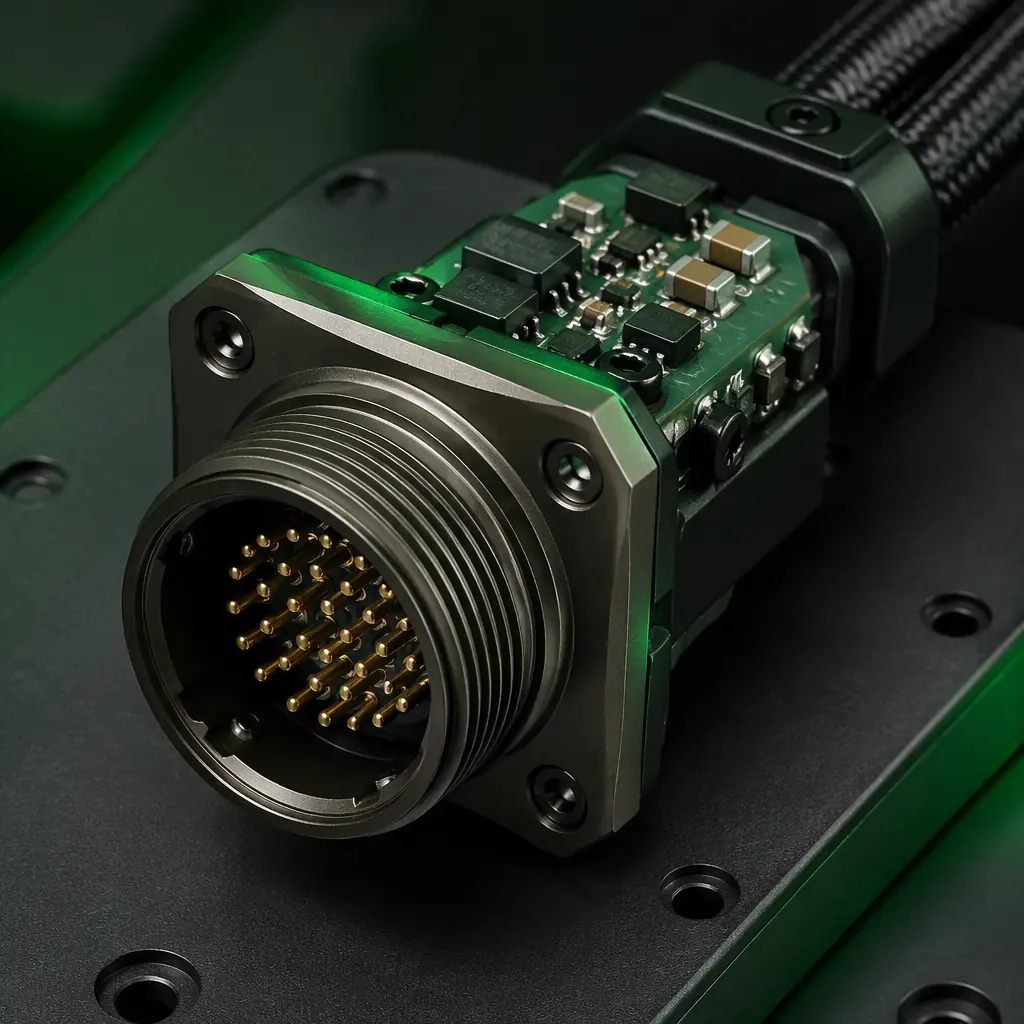 Port protection
Protecting the power path: battery, charging and USB ports
The power interfaces carry the highest energy and the most handling. A battery connector is mated and unmated hundreds of times over a platform's life, frequently in the field, by hands that just walked across a dry landing pad.
- Battery input. A TVS across the main power input, sized above the fully charged pack voltage (for 6S LiPo, V_RWM ≥ 26 V; for 12S, ≥ 51 V), clamps the mating transient. The PDB or power module should also carry a bulk capacitor to absorb the low-frequency component, the TVS handles the spike, the capacitor handles the energy.
- Charging and balance ports. Charging connectors are exposed to mains-referenced equipment and repeated handling. Unidirectional TVS plus a fuse on the charge input is the minimum; the field charging guide covers the logistics side, but the port itself needs the same protection as any handled connector.
- USB ports. USB 2.0 needs a low-capacitance (≤2 pF per line) steering-diode array on D+/D- and a TVS on VBUS. This is the single most common ESD kill on development aircraft, because the port is plugged into laptops, chargers and ground stations of unknown quality.
- Reverse-polarity and inrush. A TVS is not a reverse-polarity solution, that is a Schottky or MOSFET ideal-diode job. The two are frequently confused; the payload power budgeting guide shows how the input protection block is assembled in practice, regulator by regulator.
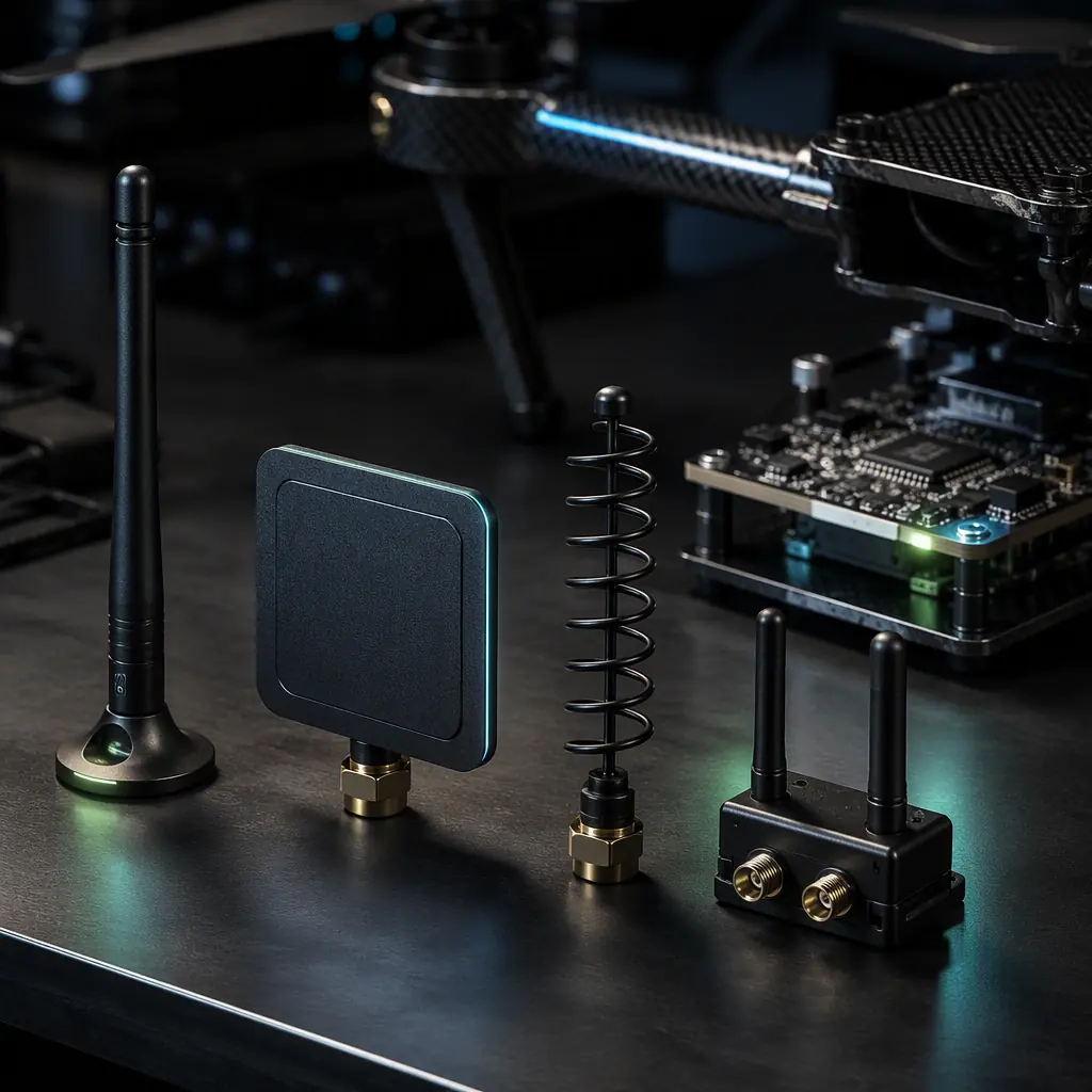
Protecting the RF and antenna ports
Antenna ports are the hardest protection problem because they carry a signal you cannot afford to load with capacitance, and the antenna itself collects charge, a carbon fiber airframe dragging through the air charges, and the discharge seeks the lowest impedance path, often the antenna feedline into the LNA.
- Low-capacitance suppression. Polymer ESD suppressors and low-cap TVS diodes rated at 0.1-0.5 pF protect the feedline without detuning the match. A 5 pF device on a 1.575 GHz GNSS feed is a visible insertion loss and a reflection; a 0.3 pF polymer is nearly invisible. The antenna selection guide quantifies how much margin the feedline has before the link budget suffers.
- Quarter-wave stub. A shorted quarter-wave stub at the operating frequency presents an open circuit to the signal but a short to DC and low frequencies, a classic GNSS and telemetry protection element that adds no insertion loss at the design frequency. At 1.575 GHz the stub is about 47 mm in air; it is a standard fixture on professional GNSS receivers.
- Lightning indirect effects. For larger airframes that operate near storms, DO-160 Section 25 (lightning indirect effects) drives protection beyond ESD: spark gaps and gas discharge tubes in parallel with the TVS handle the high-energy component. The GNSS anti-jamming guide and the RF systems guide cover the rest of the RF hardening story. The protection layer is the part that keeps the LNA alive long enough for the filters to matter.
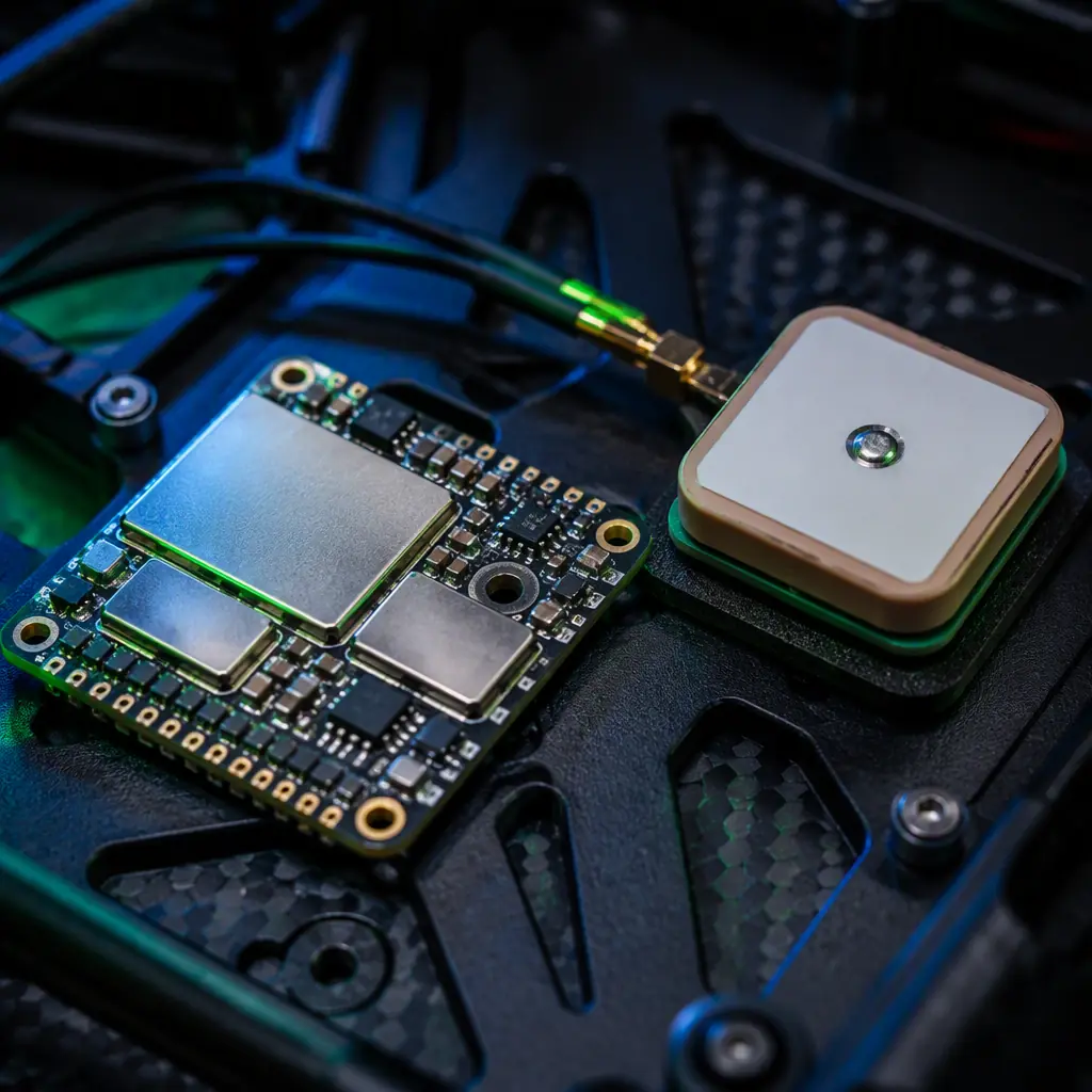 Antenna port protection
Testing and qualifying ESD protection: IEC 61000-4-2 and beyond
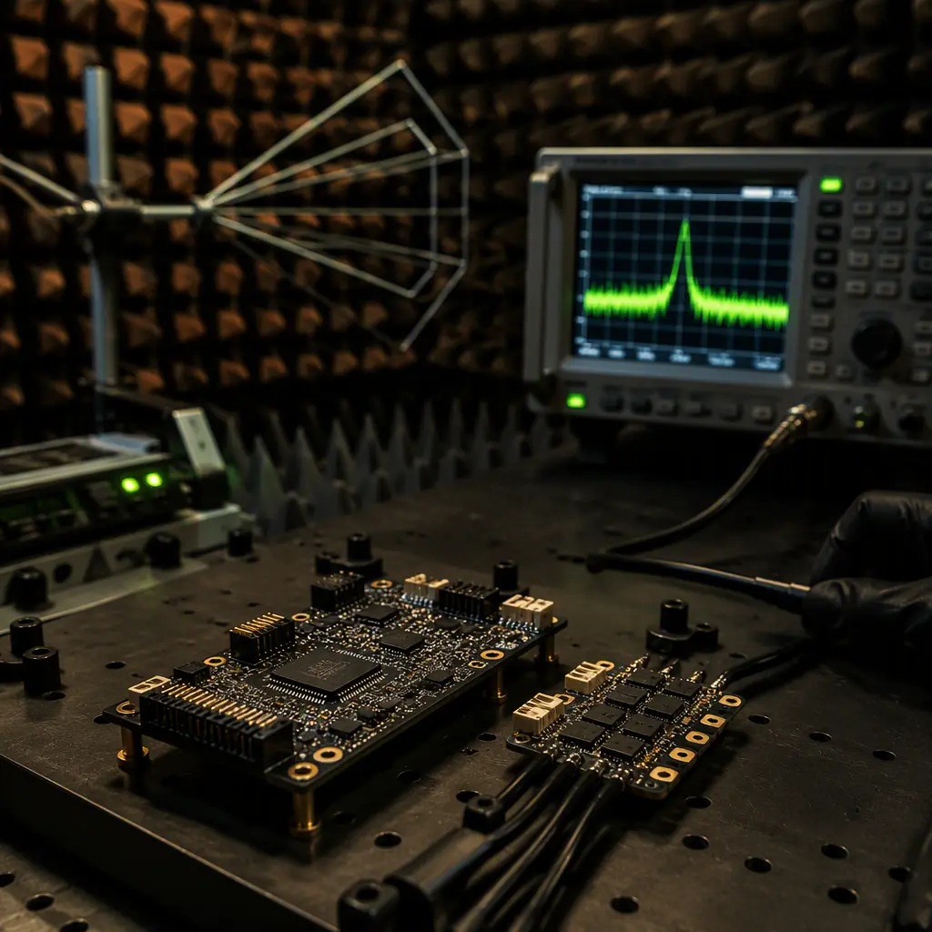
Protection is only real when it is tested at the levels the field can produce. The standard for equipment-level immunity is IEC 61000-4-2, which defines the discharge model and the test levels:
| Level | Contact discharge | Air discharge |
|---|---|---|
| 1 | 2 kV | 2 kV |
| 2 | 4 kV | 4 kV |
| 3 | 6 kV | 8 kV |
| 4 | 8 kV | 15 kV |
A UAV electronics stack destined for professional use should pass Level 4 on every externally accessible interface: contact discharge at 8 kV and air discharge at 15 kV. Component-level robustness is covered by the human-body model (HBM, typically 2 kV per JESD22-A114) and charged-device model (CDM, 500 V-1 kV per JESD22-C101), these verify the parts themselves, while IEC 61000-4-2 verifies the system design.
- Test points. Every handled interface: battery connector, payload connectors, USB, SD slot, antenna feedlines, and exposed metal bonded to ground. Each point gets contact and air discharges at both polarities.
- Pass criteria. No latch-up, no reset, no data corruption, no permanent degradation. The aircraft must continue its mission state as if nothing happened. A reset during ESD testing is a design failure, not an acceptable outcome.
- Field validation. The lab test is a snapshot; the field is the real exam. Flight logs that timestamp resets, telemetry dropouts and sensor anomalies are the monitoring layer that catches what the lab missed. The component RFP guide shows how to put the test levels and the acceptance criteria into the supplier contract so protection is provable, not promised.
 ESD-safe handling
The ESD protection procurement checklist
When the avionics stack is on the BOM, these are the clauses that make ESD protection a specification instead of an accident:
- Interface map. Every external electrical interface listed with its signal type, voltage, data rate and handling exposure, the input document for every protection decision.
- Device selection with numbers. Each protected line specified with standoff voltage, clamping voltage and maximum capacitance, not just "ESD protection included".
- Test levels. IEC 61000-4-2 Level 4 (8 kV contact / 15 kV air) on all handled interfaces, with the pass criteria written into the acceptance test.
- Layout rules. Protection within 10 mm of each connector, dedicated ground return, series resistance where applicable, the design rules that make the diodes effective.
- Handling controls. ANSI/ESD S20.20-compliant assembly and field handling, the manufacturing quality guide covers the program requirements, because design protection and handling control are complements, not substitutes.
The final rule: ESD protection is a design requirement, priced in cents and tested in kilovolts. A $0.15 TVS diode at the right connector prevents a $400 flight controller failure at the wrong moment. And on a UAV, the wrong moment is usually 100 meters up. EMS Drone ships every flight controller, ESC, radio and power module with ESD protection on every external interface, tested to IEC 61000-4-2 Level 4, with the protection schematic included in the documentation. Send the avionics interface list and the operating environment, and we will specify the protection block for the whole stack.
Explore Flight Controllers Back to Blog
Continue Reading
UAV Avionics EMC/EMI Design & Compliance
The emissions and immunity architecture that ESD protection plugs into.

UAV Electronics Manufacturing Quality
IPC-A-610 and J-STD-001 controls, including the ANSI/ESD S20.20 handling program.

UAV Connectors, Wiring & Power Distribution
The harness-side rules every protected port connects to.
UAV Antenna Selection and Placement
Where antenna feedline protection meets the link budget.

UAV GNSS Anti-Jamming & Spoofing
RF hardening on the positioning side, from the feedline up.